Change Via Template Of All Vias Altium
Change Via Template Of All Vias Altium - Selected pad (s) or via (s) can then be edited to use a different template in. Altium has a convenient, but little bit hidden instrument for bunch changing of hole sizes. Changing free pads to vias can be useful when. Creating a pad or via template. In this blog post, we'll walk you through the process of designing vias using altium designer, from the basics to advanced techniques. For example, if i decided after routing a few traces that. I've configured the routingvias rule to have the hole size and. 55k+ customers worldwide35+ years of excellence In this article, we will go over the fundamentals of via design using altium designer electronic design automation software. How do you configure the vias that appear when you're dragging out a track on the pcb and change layers? It will select all vias of that size/diameter. The new value you enter will be applied to. 55k+ customers worldwide35+ years of excellence Creating a pad or via template. Changing free pads to vias can be useful when. In this article, we will go over the fundamentals of via design using altium designer electronic design automation software. For example, if i decided after routing a few traces that. Selected pad (s) or via (s) can then be edited to use a different template in. To define a new via type, switch to the via types tab of the layer stack manager. Use the pad & via templates mode of the pcb panel to locate and select a pad or via of interest. When designing an adapter pcb or any other type of pcb using altium designer, it is crucial to understand the correct usage of vias to achieve the desired results. A free pad is one that is not part of a parent component object. How do you set the size of a via in altium. Creating a pad or via template.. Creating a pad or via template. Selected pad (s) or via (s) can then be edited to use a different template in. It will select all vias of that size/diameter. Altium has a convenient, but little bit hidden instrument for bunch changing of hole sizes. Use the pad & via templates mode of the pcb panel to locate and select. In this article, we will go over the fundamentals of via design using altium designer electronic design automation software. Selected pad (s) or via (s) can then be edited to use a different template in. A free pad is one that is not part of a parent component object. In this blog post, we'll walk you through the process of. How do you set the size of a via in altium. 55k+ customers worldwide35+ years of excellence I've configured the routingvias rule to have the hole size and. Use the pad & via templates mode of the pcb panel to locate and select a pad or via of interest. Changing free pads to vias can be useful when. How do you set the size of a via in altium. Changing free pads to vias can be useful when. Use the pad & via templates mode of the pcb panel to locate and select a pad or via of interest. Creating a pad or via template. It will select all vias of that size/diameter. How do you configure the vias that appear when you're dragging out a track on the pcb and change layers? To define a new via type, switch to the via types tab of the layer stack manager. In this blog post, we'll walk you through the process of designing vias using altium designer, from the basics to advanced techniques. 55k+. How do you configure the vias that appear when you're dragging out a track on the pcb and change layers? Use the pad & via templates mode of the pcb panel to locate and select a pad or via of interest. Altium has a convenient, but little bit hidden instrument for bunch changing of hole sizes. In this article, we. To define a new via type, switch to the via types tab of the layer stack manager. When designing an adapter pcb or any other type of pcb using altium designer, it is crucial to understand the correct usage of vias to achieve the desired results. I've been working with circuit studio for a board design, and i haven't been. In this article, we will go over the fundamentals of via design using altium designer electronic design automation software. When designing an adapter pcb or any other type of pcb using altium designer, it is crucial to understand the correct usage of vias to achieve the desired results. It will select all vias of that size/diameter. Selected pad (s) or. To define a new via type, switch to the via types tab of the layer stack manager. In this blog post, we'll walk you through the process of designing vias using altium designer, from the basics to advanced techniques. It will select all vias of that size/diameter. In this article, we will go over the fundamentals of via design using. I've configured the routingvias rule to have the hole size and. Changing free pads to vias can be useful when. Creating a pad or via template. Selected pad (s) or via (s) can then be edited to use a different template in. The new value you enter will be applied to. In this blog post, we'll walk you through the process of designing vias using altium designer, from the basics to advanced techniques. I've been working with circuit studio for a board design, and i haven't been able to figure out how to change settings on a group at a time. Use the pad & via templates mode of the pcb panel to locate and select a pad or via of interest. How do you configure the vias that appear when you're dragging out a track on the pcb and change layers? 55k+ customers worldwide35+ years of excellence When designing an adapter pcb or any other type of pcb using altium designer, it is crucial to understand the correct usage of vias to achieve the desired results. I have got a draft boards with some vias different vias, so let's look at the all existing. In this article, we will go over the fundamentals of via design using altium designer electronic design automation software. How do you set the size of a via in altium. For example, if i decided after routing a few traces that.
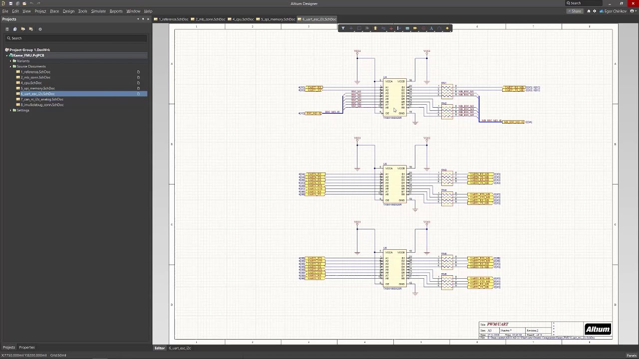
How To Change Via Types In Altium
Altium Designer Schematic Template Altium Edit Schematic Tem
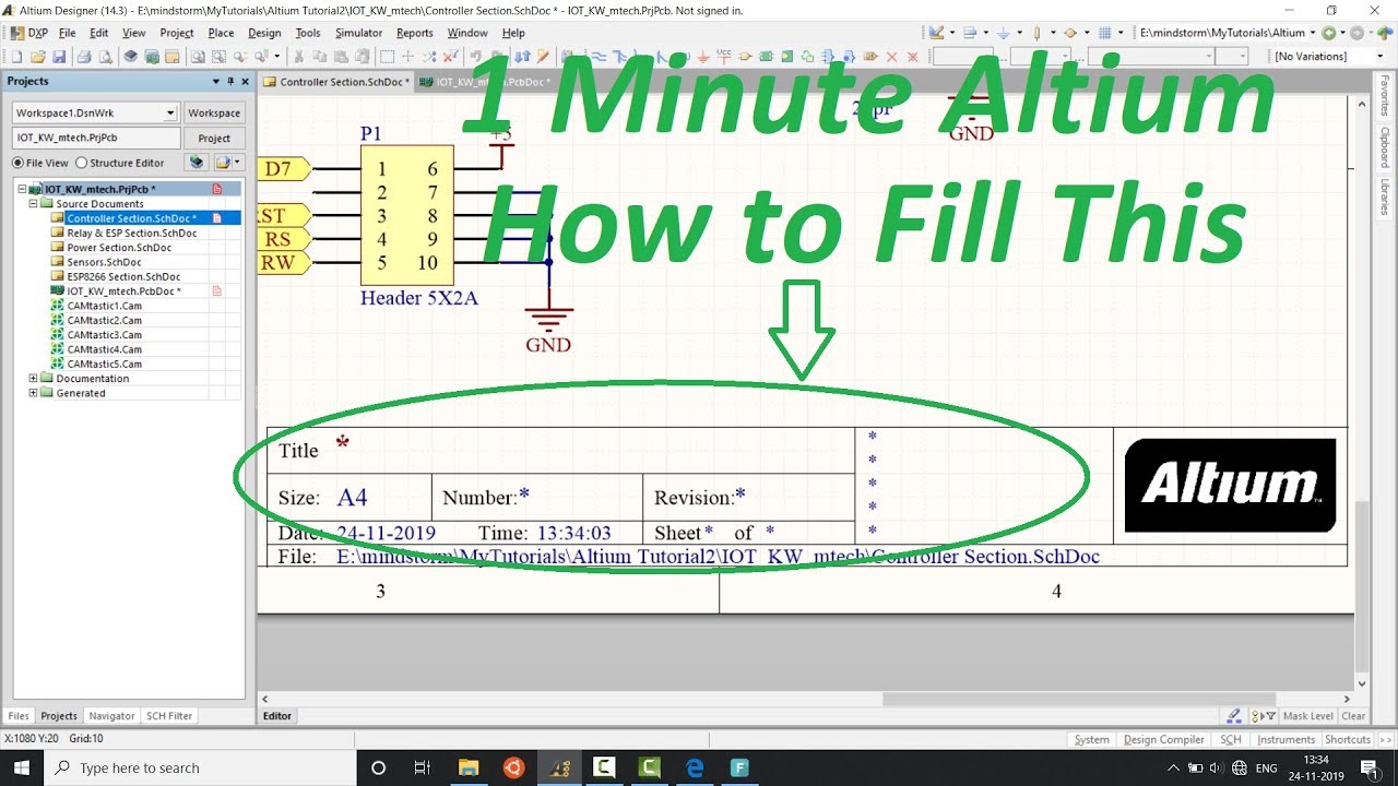
Altium Schematic Title Block Template Altium Schematic Creat
Pad and Via Templates with Altium Designer YouTube

Altium Place Via Shortcut

pcb design Altium Single Layer Mode Vias Color Electrical

Altium Designer Tutorial Working with vias and multiple layers YouTube
PCB Via Design Using Altium Designer Sierra Circuits

Altium Designer 15.1 Pad & Via Libraries YouTube

Youtube Altium 2923 Schematic Symbol Altium Designer 21
A Free Pad Is One That Is Not Part Of A Parent Component Object.
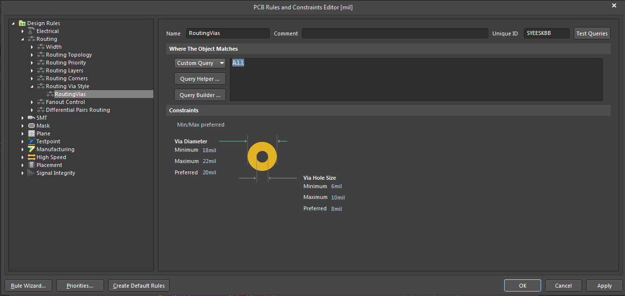
It Will Select All Vias Of That Size/Diameter.
To Define A New Via Type, Switch To The Via Types Tab Of The Layer Stack Manager.
Altium Has A Convenient, But Little Bit Hidden Instrument For Bunch Changing Of Hole Sizes.
Related Post: